applications
what do we research and manufacture?
Testing of the properties and structure of materials

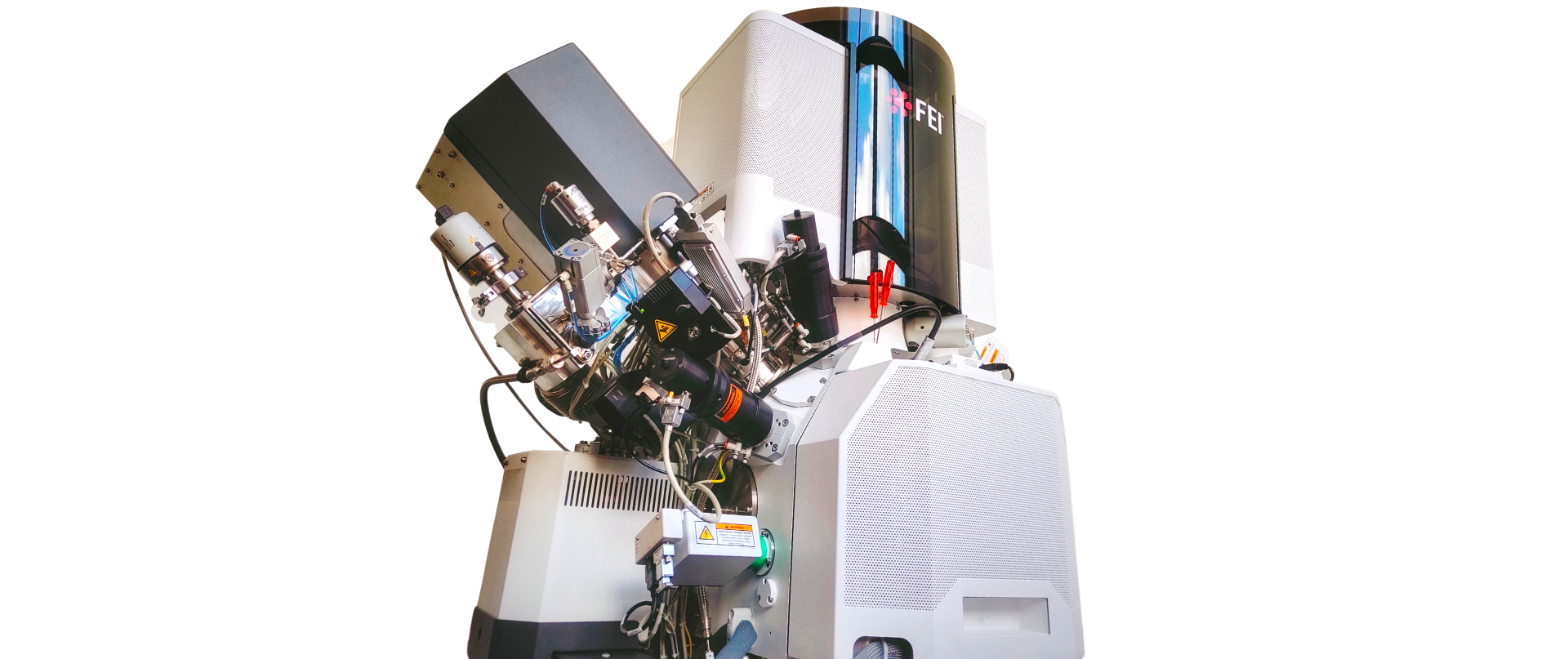
We verify the key properties of materials and their structure using basic laboratory techniques such as metallographic tests and hardness measurements, as well as advanced imaging methods like scanning and transmission electron microscopy (SEM, TEM) or atomic force microscopy (AFM). Scanning electron microscopy (SEM) is an excellent technology that allows imaging the sample surface at a micro- and nanometric scale, achieving the magnification of up to 1,000,000 times and visualizing its topography or structure. Observations made with a number of specialist detectors provide a comprehensive set of information, e.g. distribution of elements obtained by EDS/EDX microanalysis of chemical composition. Moreover, the microscopes used in the research are built in a dual beam microscope configuration, which allows for making precise local cross-sections through the tested elements, up to several hundreds μm depending on the material, making their inner microstructure visible.
Thin films testing

Many industries see the application of specialized coatings in a wide range of complexities and forms. A common critical feature of coatings is their thickness and chemical composition, which often need to meet strict requirements of manufacturers. These parameters translate directly into the quality and reliability of manufactured components. For specialized coatings made of precious and semiprecious metals, their thickness must be strictly controlled within certain ranges. The measurements of coating thickness offered by Nanores Lab allow for precise determination of coating thickness at a location specified by the client. High-resolution imaging mode allows for multi-layer coating measurement starting from 10 nm thickness.
Lithium-ion batteries testing

Comparing to other battery technologies available on the market, lithium-ion batteries are highly efficient energy storage devices, and demand for them continues to grow. Safer, stronger, more economical batteries are now one of development challenges of the future. Nanores Lab offers a number of tools for identification and analysis of defects, faults and failures. By combining analytical techniques such as microcomputed tomography (microCT), scanning and transmission electron microscopy (SEM and TEM), as well as focused ion beam technology (FIB) scientists, engineers and technologists can gain valuable structural and chemical information that they need to improve their processes.
Semiconductors testing

Semiconductor industry continues to develop and the state-of-the-art semiconductor devices are not only getting smaller than their precursors, but also more complex. As a result, they require more sophisticated tools needed for development, prototyping, identification and control of defects, as well as making precise and high-resolution microscopic observations. Scanning electron microscopy (SEM) in combination with focused ion beam (FIB) is a perfect technique that offers high-precision analytical capabilities.
If you are interested in a given application, we invite you to a 4-hour test day.
Quality control

Products are becoming more complex, as are the demands placed on them, so a fast, in-depth and multifactor quality control is essential for process management. Thanks to a comprehensively equipped laboratory and a team of experts, complex problems related to damage analysis and determining its root causes can be easily identified and solved.
Defect analysis

Even small defects can have a significant impact on the safety and performance of the final product. The slightest crack or contamination can not only reduce the quality and durability of the product, but also cause disastrous failures. Performing metallographic tests and hardness measurements is often the first step to identify the cause of a defect. Some applications and defect cases require the use of electron microscopy techniques. SEM offers magnification and depth of field required for detailed fault analysis and failure identification. It also provides a lot of information to precisely characterize the damage and identify its root cause.
Prototyping

Using our specialist equipment, as well as knowledge and experience, we are able to offer the services of structure prototyping in the following areas: micro- and nanoelectronics (NEMS, MEMS), automatics (micro- and nanofluidics), optics (photonic crystals, micro- and nanolenses) and many others.
Micro- and nanocomponents production

The manufacture of components at the micro- and nano-scale is a subject of the increasing interest around the world, both in academia and industry. Such components require high precision, repeatability and thorough quality control already at the production stage. Using the high-class equipment, methods and experience of our experts, we are able to manufacture precise components for such industries as: electronics and photonics, optics, automatics, and many others.