testing methods
what testing methods do we offer?
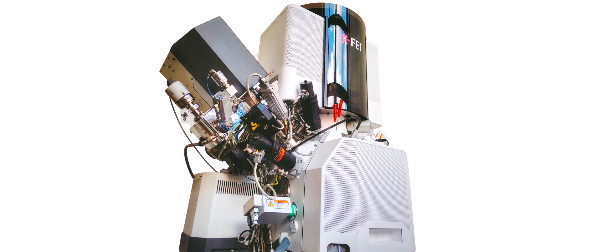
Surface testing (SEM)
Scanning electron microscope (SEM) images provide information about the morphology or topography of a sample, fracture or polished section. They also allow for the observation and identification of defects even of sub-micron sizes, the measurement of size of grains, pores or other details on the surface. The results of such analyzes provide valuable information to companies and research entities from many industries, such as electronics, chemical, ceramics, metallurgy and many others.
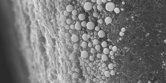
Cross-section tests (SEM/Xe-PFIB/Ga-FIB)

During these tests, a local cross-section is created, the surface of which is polished with an ion beam. This allows for the cross-sectional area analysis of the tested object using electron and ion microscopy techniques. These tests are perfect for analyzing the quality of sinters, welds and multi-layer structures (e.g. integrated circuits or anti-reflective coatings).
EDS elemental analysis

During electron beam imaging, the preparation atoms emit characteristic X-rays that are unique to each element. An advanced EDS detector collects this signal and performs elemental analysis pointwise, linearly or on the surface. It is possible to create a map that shows the identified elements arrangement from 4Be to 95Am in a given area of the analyzed sample.
METALLOGRAPHIC EXAMINATION
Metallographic studies enable the analysis of the internal structure of metallic materials, composites, electronics, plastics, and ceramics using optical and scanning electron microscopy. This methodology enables a deeper understanding and characterization of the inner structure of materials, a crucial aspect across various scientific and industrial domains. The primary objective of metallographic investigations is to identify, describe, and gain insight into the microstructure of the material.
During the research, the structure of the material, its components, their arrangement, as well as the assessment of the quality and homogeneity of the material are determined. Metallographic examinations enable the detection of potential defects, inclusions, non-uniformities, or microcracks that could affect the strength or functional properties of the material.
COMPLEMENTARY METHODS
Furthermore, our laboratory complements metallographic examinations with specialized techniques such as scanning electron microscopy (SEM), focused ion beam (FIB), microanalysis of chemical composition (EDS), transmission electron microscopy (TEM), and hardness measurements.
Photo
HARDNESS MEASUREMENTS
APPLICATIONS
- HD | NHD (Nht) | SHD (Rht) measurement;
- 2D | 3D hardness graphs;
- Customizable hardness distributions;
- Measurement of resistance to brittle fracture KIC.
MEASUREMENT METHODS AND RANGES
- Vickers hardness measurement according to PN-EN ISO 6507-1 standard in the HV0.01 – HV150 load range;
- Brinell hardness measurement according to PN-EN ISO 6506-1 standard in the HBW 2.5/6.25 – HBW 2.5/187.5 load range;
- Rockwell hardness measurement according to PN-EN ISO 6508-1 standard in the HRC scale range;
- Case hardness depth (CHD) measurement according to PN-EN ISO 2639 or PN-EN ISO 18203 standard;
- Nitriding hardness depth (NHD | Nht) measurement according to DIN 50190-3 standard;
- Surface hardness depth (SHD | Rht) measurement according to DIN 10328 (PN-EN 10328) standard.
Photo
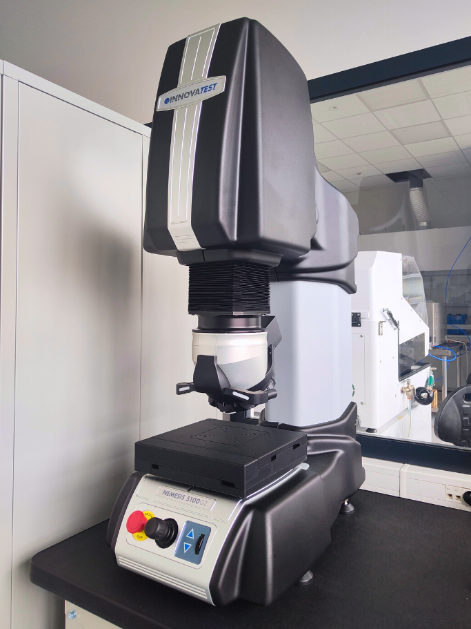
Hardness measurements are crucial and fundamental material tests that allow for the determination of their resistance to plastic deformation and scratching. The laboratory is equipped with a hardness tester that enables the use of popular measurement methods such as Vickers, Brinell, and Rockwell over a wide range of loads from 0.01 kgf to 250 kgf. This versatility enables us to customize measurement techniques to suit specific applications and material hardness levels, thus aiding in the precise evaluation of material mechanical properties and quality.
TEM sample preparation

Our offer includes manufacturing extremely thin samples (lamellas) intended for tests using Transmission Electron Microscopy (TEM). The sample thickness that is guaranteed by us is below 100 nm (depending on the material, the sample thickness may even be less than 20 nm). The lamellas are prepared by us from the sample area indicated by the client, polished and ready for TEM observation. The Xe-PFIB technology, due to xenon ions usage, enables the preparation of samples that are incompatible with Ga-FIB technology, including aluminum samples or samples containing gallium.
If you are interested in a given application, we invite you to a 4-hour test day.
Environmental SEM analysis

Owing to controlled vacuum, environmental SEM imaging allows for testing biological and other preparations that begin to gas under high vacuum conditions. In this mode, we can control humidity and temperature. As a result, various materials can be introduced into the microscope chamber without the need to dry them. These can be samples in liquid and solid form, highly humid samples, and all samples incompatible with high vacuum, e.g. plant and animal tissues.
MiBot Manipulators

Manipulators driven by piezoelectric actuators allow for small electronic circuits and components to be tested and moved with nanometric precision. A set of two MiBot devices, coupled with a scanning electron microscope or a laser confocal microscope, allows for research and testing of submicron elements. Moreover, in combination with external measuring electronics, it enables the determination of resistance and current-voltage characteristics of microelectronic devices, or semiconductor damage analysis.
Laser processing (femtosecond laser)

Our workstation can cut difficult materials, e.g. ceramics, diamonds or hardened glass. It is suitable for micro-processing and micro-components production. It is also widely applied in the processing of optical elements (photonic crystals, fiber-optic cables, micro-lenses) and micro-electro-mechanical systems (MEMS). It is used, for example, for drilling micro-holes with profiled, smooth edges, cutting out elements or materials marking.
3D Reconstruction (SEM/Xe-PFIB/Ga-FIB)

With our advanced devices and professional software, we are able to perform cross-sections series and then record them in a micro- and nanometric scale. The results of this process can then be transformed into high-quality 3D reconstructions of the sample microstructure. This enables the structural changes verification and their statistical analysis within a certain sample volume.
Surface testing (AFM)

Surface testing using an atomic force microscope is an ideal method of examining the materials roughness and verifying the correctness of the processes of applying all layers at any production stage.