Nanotechnology laboratory equipment
what microscopes do we use?
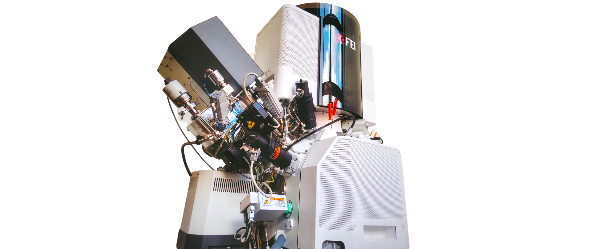
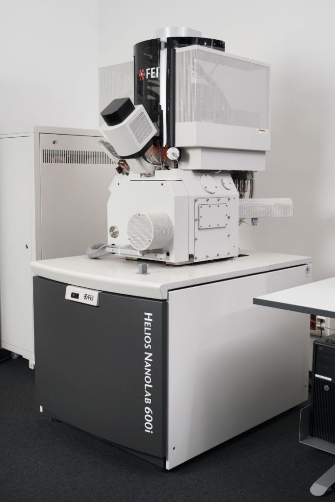
SEM/Ga-FIB FEI Helios NanoLab 600i microscope
The FEI dual beam SEM/Ga-FIB microscope combines the advantages of an ultra high-resolution electron microscope and an ion microscope. It can therefore be used for high-resolution imaging and as a material processing tool. The energy of the focused beam of gallium ions allows for the preparation material to be selectively removed and modified at the nanoscale. This is related to the possibility of making cross-sections, 3D reconstruction and TEM samples preparation, as well as prototyping processes in nano- and microscale. Available detectors: ETD, TLD, CBS and EDS.
* To get more detailed information, please contact our engineers.
Applications
- The ultra-high-resolution imaging of surface preparation.
- Creation and analysis cross-sections in nano- and microscale.
- Selective application of materials in FEBID and FIBID technology.*
- Imaging contrast material preparation.
- The ability to characterize a wide range of formulations of conductive and non-conductive without modifying them.*
- Three-dimensional reconstruction of the specimen on the basis of SEM images (approximately 1 000 µm3 volume).
- Preparation of high-quality TEM samples with a thickness of less than 100 nm.
- Rapid prototyping of spatial structures in nano- and microscale.
Parameters
Landing voltage range:
- electron beam: 350 V – 30 kV (50 V – 30 kV with Beam Deceleration mode),
- ion beam: 500 V – 30 kV.
Resolution:
- electron beam: 1 nm,*
- ion beam: 2,5 nm.*
Maximum sample size:
- diameter: 150 mm diameter with full rotation (assembly possible of larger preparations*),
- height: 100 mm,
- weight: 500 g (including the sample holder).
Detectors
- ETD (secondary electrons)
- TLD (secondary electrons)
- ICE (secondary ions)
- CBS (backscattered electrons)
Photo
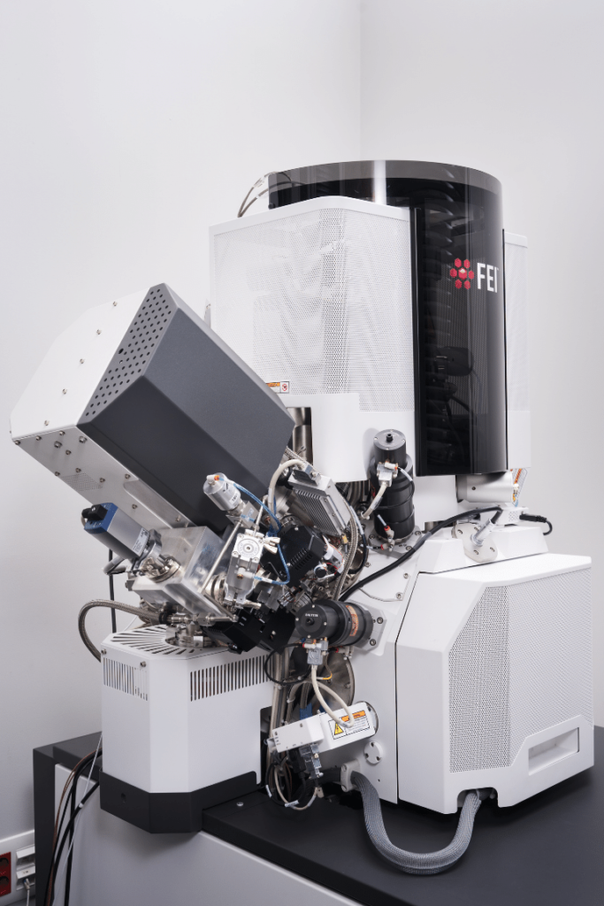
SEM/Xe-PFIB FEI Helios G4 PFIB CXe microscope
Helios G4 PFIB CXe is a dual beam microscope with an electron column and an ion column that generates a xenon ions beam. Xenon plasma focused ion beam (Xe-PFIB) technology allows for new tests, unattainable by other methods. In combination with an ultra-high-resolution electron microscope and a fast EDS detector from Bruker, it is the only such analytical system commercially available in Poland. It is distinguished, among others, by up to 50 times faster work than in the case of gallium technology (Ga-FIB), no ion implantation and compatibility with most materials – including aluminum samples and gallium-containing samples. Available detectors: ETD, TLD, ICE, ICD and EDS.
* To get more detailed information, please contact our engineers.
Applications
-
The ultra-high-resolution imaging of surface preparation.
-
Create maps of elemental EDS, analysis of point and linear elemental composition.
-
Creation and analysis cross-sections in nano- and microscale.
-
Selective application of materials in FEBID and FIBID technology.*
-
Imaging contrast material preparation.
-
The ability to characterize a wide range of formulations of conductive and non-conductive without modifying them,*
-
Three-dimensional reconstruction of the specimen on the basis of SEM images (approximately 1 000 µm3 volume).
-
Preparation of high-quality TEM samples with a thickness of less than 100 nm – compatibility with the materials based on aluminum and gallium.
-
Rapid prototyping of spatial structures in nano- and microscale.
-
Etching material without leaving artifacts (e.g. implanting gallium).
Parameters
Landing voltage range:
- electron beam: 50 V – 30 kV,
- ion beam: 2 kV – 30 kV.
Resolution:
- electron beam: 1 nm,*
- ion beam: <25 nm.*
Maximum sample size:
- diameter: 150 mm diameter with full rotation (assembly possible of larger preparations*),
- height: 100 mm,
- weight: 500 g (including the sample holder).
Detectors
-
ETD (secondary electrons)
-
TLD (secondary electrons)
-
CBS backscattered electrons)
-
ICE (secondary ions)
-
EDS (characteristic X-rays*)
Photo
Quanta 3D 200i ESEM/Ga-FIB microscope
Quanta 3D 200i ESEM/Ga-FIB microscope combines an electron microscope, based on a tungsten cathode, and an ion microscope. Its great advantage is the possibility of using three imaging modes: high vacuum (Hi-Vac), low vacuum (Lo-Vac) and environmental (ESEM). Depending on the sample type, the microscope’s resolving power is estimated at approx. 300–500 nm. In the low vacuum mode (Lo-Vac), images of dry non-conductive samples can be obtained without any pre-preparation. On the other hand, environmental SEM – due to the controlled vacuum – allows for the testing of biological and other preparations that begin to gas under high vacuum conditions. These can be samples in liquid and solid form, highly humid samples, and all samples incompatible with high vacuum, e.g. plant and animal tissues. Available detectors: ETD, BSE, LFD for Low Vac and GSED for ESEM mode.

Olympus LEXT 3D Measuring Laser Microscope OLS5000-SAF confocal microscope
The Olympus LEXT 3D confocal microscope allows for precise measurement of shape and surface roughness of samples at the submicron level. Performing accurate 3D measurements on a wide range of sample types, it provides reliable data needed to ensure the quality and control of manufacturing processes. At the same time, this microscope offers the imaging of the microstructure of materials, which allows for basic verification of the material compliance with requirements – including the analysis of potential defects such as non-metallic inclusions, microcracks, porosity or other material discontinuities.

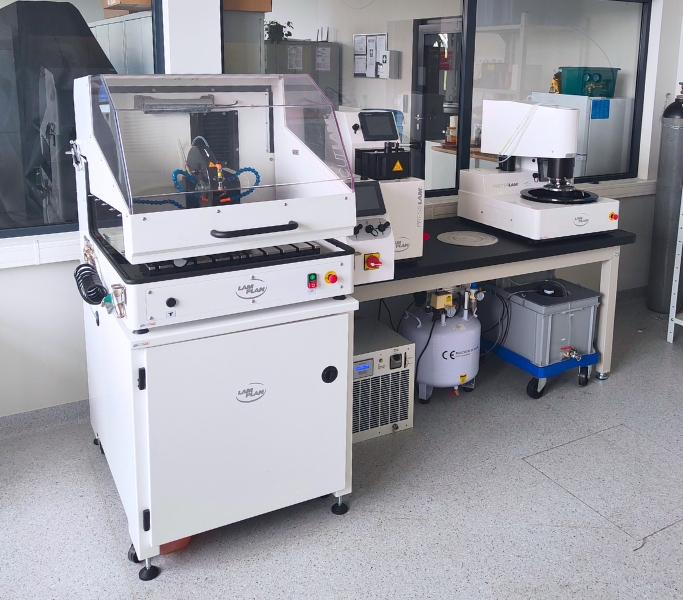
METALLOGRAPHIC LABORATORY SETUP
Our advanced laboratory setup facilitates the preparation of material samples for in-depth analysis. We have the capability to perform imaging using various techniques, including laser confocal microscopy, optical microscopy, scanning and transmission electron microscopy, as well as atomic force microscopy. These techniques enable the assessment of surface quality and the evaluation of microstructure morphology across a wide range of scales, from the nano to the macro level.
Applications
- Qualitative analysis of microstructure.
- Identification of material defects.
- Identification of technological processes conducted on the tested component.
- Evaluation of graphite nodules in terms of shape, distribution, and size.
- Measurement of coating thickness using metallographic and scanning electron microscopy methods.
- Assessment of non-metallic inclusions.
- Grain size evaluation.
- Measurement of carburization/nitridation depth using metallographic methods.
- Measurement of surface-hardened layer thickness using metallography.
EQUIPMENT COMPONENTS
- Metallographic cutter.
- Hot mounting device.
- Metallographic grinding and polishing machine.
- Metallographic electro-polishing machine.
- DM2700 Leica metallographic microscope.
Photo
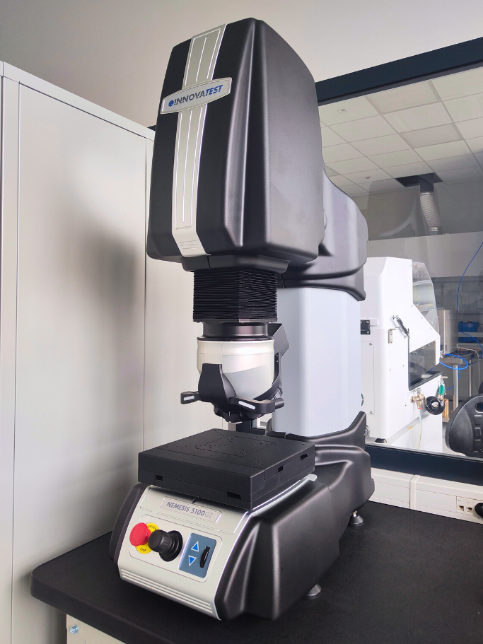
NEMESIS 51000G2/A HARDNESS TESTER
The fully automated NEMESIS 51000G2/A hardness tester allows for measurements using Brinell, Vickers, and Rockwell methods within the load range of 0.010 kgf to 250 kgf. It is a significant tool for evaluating the strength and mechanical properties of materials.
Applications
- HD | NHD (Nht) | SHD (Rht) measurement;
- 2D | 3D hardness graphs;
- Customizable hardness distributions;
- Measurement of resistance to brittle fracture KIC.
MEASUREMENT METHODS AND RANGES
- Vickers hardness measurement according to PN-EN ISO 6507-1 standard in the HV0.01 – HV150 load range;
- Brinell hardness measurement according to PN-EN ISO 6506-1 standard in the HBW 2.5/6.25 – HBW 2.5/187.5 load range;
- Rockwell hardness measurement according to PN-EN ISO 6508-1 standard in the HRC scale range;
- Case hardness depth (CHD) measurement according to PN-EN ISO 2639 or PN-EN ISO 18203 standard;
- Nitriding hardness depth (NHD | Nht) measurement according to DIN 50190-3 standard;
- Surface hardness depth (SHD | Rht) measurement according to DIN 10328 (PN-EN 10328) standard.
Photo
Laser workstation
The unique laser workstation constructed by our team from independent elements consists of a femtosecond laser, a five-axis head (operating, among others, in the trepanation mode) and a movable table increasing the production capacities of even very complex geometries. Its advantages include also the minimization of thermal interactions in the processed material, allowing for very precise and clean work, without the need for further processing. It is suitable for micro-processing and micro-components production. It is also widely applied in the processing of optical elements (photonic crystals, fiber-optic cables, micro-lenses) and micro-electro-mechanical systems (MEMS).